Contact mechanics in nanoscale patterning
Patterning materials at the micrometer and nanometer scales is essential to semiconductor manufacturing, displays and flexible electronics. As features shrink, projection photolithography becomes increasingly diffraction-limited and expensive, and many patterning processes instead rely on mechanical contact to deform a material: nanoimprint lithography, gravure and flexographic printing, and transfer processes that exploit rate-dependent adhesion. What these processes have in common is that the patterns are many orders of magnitude larger in lateral extent than the thickness of the film being patterned. That makes them well suited to Green’s-function and boundary-element methods, which describe a surface or film by its deformation in response to a localized load, and which make it computationally affordable to simulate chip-scale and larger designs.
Nanoimprint lithography (NIL) process modeling
In NIL, a nanopatterned stamp or template deforms a thermoplastic polymer or UV-curing resin to transfer a design to a substrate such as a silicon wafer. NIL can lower patterning costs substantially, but it exhibits strong, systematic pattern dependences: templates with large or varied feature sizes, shapes or densities deflect elastically during imprinting, and the resulting variations in residual-layer thickness, incomplete cavity filling and etch depth propagate to critical device dimensions. Without a predictive model, process development has been highly experimental, and a systematic, layout-driven defect could mean remaking a template at a cost often exceeding $100K.
Our simulation approach borrows analytical point-load response functions of the kind developed for contact problems in tribology. The stamp is represented by its elastic response to a localized load and the resist by thin-film viscous flow, and an iterative algorithm finds the evolving contact-pressure distribution between them, from which the deformed resist shape follows directly. The method is at least 1000 times faster than finite-element simulation and lets complex chip-scale layouts be abstracted simply, so that numerical simulation becomes a practical way to evaluate a layout for NIL. The framework has been extended to capture the surface tension of the imprinted material, directional effects in roller-based imprint, and droplet-dispensed UV-NIL at feature, droplet and template scales.
The same mechanics supports design. Backside grooves can raise a stamp’s bending compliance to absorb wafer nanotopography, and a computational framework for two-layered elastic stamps (a Journal of Applied Physics Featured Article) shows how stamp architecture can equalize residual-layer thickness while conforming to rough or curved substrates; the same framework applies to microcontact printing and to manufacturable, micropatterned dry adhesives. A simple razor-blade test measures the energy needed to demold a stamp.
Simprint Nanotechnologies
The simulation technique is the subject of two issued US patents and received the 2009 Software in Design Innovation Award from the Institution of Engineering and Technology. It was spun out in 2010 as Simprint Nanotechnologies, whose software was used by Canon and by Toshiba Memory (now Kioxia) to guide the early development of NIL processes for manufacturing NAND flash memory. Interest in NIL has since grown again for producing metasurfaces, metalenses and optical waveguides for augmented- and virtual-reality hardware, where spatially varied nanopatterns make fast process modeling especially valuable.
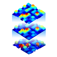
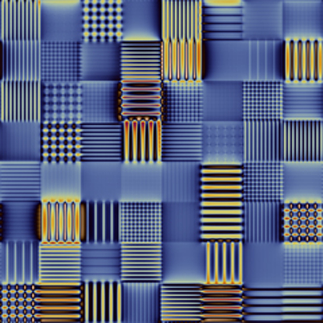
Banner: simulated pattern-dependent residual-layer thickness and stamp deflection for nanoimprint test layouts.
Key publications
[J28] H.K. Taylor and R.D. O’Rorke, “A computational design framework for two-layered elastic stamps in nanoimprint lithography and microcontact printing”, Journal of Applied Physics, vol. 125, 094901, 2019. doi: 10.1063/1.5081495. Selected as a Featured Article: see the AIP Scilight about the work.
[J14] H.K. Taylor, “Simulation and mitigation of process and pattern dependencies in nanoimprint lithography”, Journal of Photopolymer Science and Technology, vol. 24, no. 1, pp. 47-55, 2011. doi:10.2494/photopolymer.24.47 (Accompanying an invited talk at the Photopolymer Science and Technology Conference, Chiba, Japan, June 2011).
[J12] H.K. Taylor, D.S. Boning, and C. Iliescu, “A razor-blade test of the demolding energy in a thermoplastic embossing process”, Journal of Micromechanics and Microengineering, vol. 21, 067002, 2011. doi:10.1088/0960-1317/21/6/067002
[J11] H.K. Taylor, K. Smistrup, and D.S. Boning, “Modeling and simulation of stamp deflections in nanoimprint lithography: exploiting backside grooves to enhance residual layer thickness uniformity”, Microelectronic Engineering, vol. 88, pp. 2154-2157, 2011. doi:10.1016/j.mee.2010.12.090 (presented at Micro- and Nano-Engineering, Genoa, Italy, Sep. 2010: abstract .pdf | poster .pdf)
[NC23] H.K. Taylor, “Defectivity prediction for droplet-dispensed UV nanoimprint lithography, enabled by fast simulation of resin flow at feature, droplet, and template scales”, Proc. SPIE, vol. 9777, 97770E, 2015. (invited) doi:10.1117/12.2218757
[NC22] H.K. Taylor, “Enabling layout and process optimization with fast, full-field simulation of droplet-dispensed UV-NIL”, presented at Nanoimprint and Nanoprint Technology, Napa, CA, Oct. 2015 (invited). abstract .pdf | presentation .pdf
[C4] H.K. Taylor, “Fast Simulation of Pattern Formation and Process Dependencies in Roller Nanoimprint Lithography”, presented at Materials Research Society Fall Meeting, Boston, MA, Nov. 2012. doi:10.1557/opl.2013.49
[NC14] H.K. Taylor, “Simulation of roll-to-roll and roll-to-plate NIL: modeling the effects of process speed, imprinting load, roller elasticity, and pattern design”, presented at Nanoimprint and Nanoprint Technology, Napa, CA, Oct. 2012. abstract .pdf
[NC13] H.K. Taylor and E.J. Wong, “Fast simulation of nanoimprint lithography: modeling capillary pressures during resist deformation”, presented at Nanoimprint and Nanoprint Technology, Jeju, Korea, Oct. 2011. abstract .pdf
[NC12] D.S. Boning, A.B. Kahng, H.K. Taylor, and Y.-K. Wu, “Chip-scale simulation of residual layer thickness uniformity in thermal nanoimprint lithography: evaluating stamp cavity-height and ‘dummy-fill’ selection strategies”, presented at Nanoimprint and Nanoprint Technology, Copenhagen, Denmark, Oct. 2010. abstract .pdf | presentation .pptx
[NC11] H.K. Taylor, K. Smistrup, and D.S. Boning, “Modeling the enhancement of nanoimprint stamp bending compliance by backside grooves: mitigating the impact of wafer nanotopography on residual layer thickness”, presented at Nanoimprint and Nanoprint Technology,Copenhagen, Denmark, Oct. 2010. abstract .pdf | poster .pdf
[NC10] H.K. Taylor and D.S. Boning, “Towards nanoimprint lithography-aware layout design checking”, Proc. SPIE, vol. 7641, 764129, 2010. doi:10.1117/12.846499 | presentation .pdf
[NC9] H.K. Taylor and D.S. Boning, “Fast simulation of pattern dependencies in thermal nanoimprint lithography”, presented at Nanoimprint and Nanoprint Technology, San Jose, CA, Nov. 2009. abstract .pdf | presentation .pdf
[P2] H.K. Taylor and D.S. Boning, “Method and Apparatus for Embossing a Deformable Body”, US Patent 8,585,954, issued 19 November, 2013.