Diffractive inline optical metrology
Hot embossing and imprinting of thermoplastics are attractive ways to manufacture micro- and nanofluidic devices at low cost, from wafer-sized pieces to continuous reels. Producing such devices at scale needs fast, non-destructive ways of checking on the production line whether pattern replication is complete: whether channels have been embossed to the right depth, have collapsed during bonding, or were incompletely filled. Scanning-probe and interferometric methods can measure these features, but they are slow and usually need the part to leave the line.
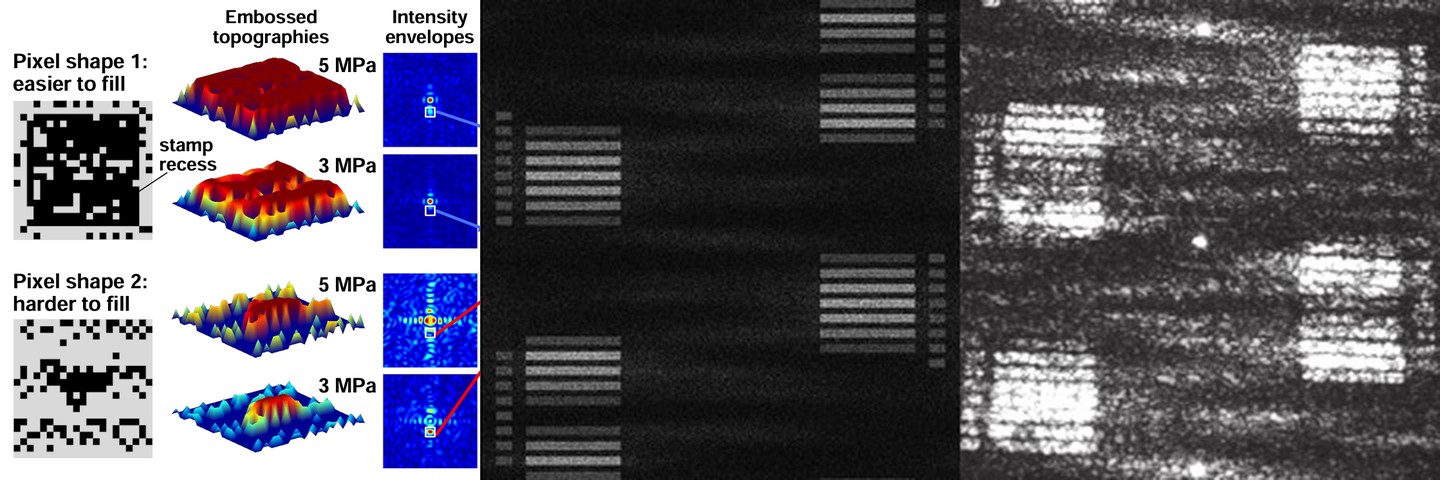
We explored using the diffraction of light instead. In one scheme, the embossed part is placed in contact with a row of nine phase-relief holograms, designed by simulated annealing, and the combination is illuminated with a laser. The far-field diffraction patterns are then read with a series of simple binary intensity comparisons, which reveals the approximate depth of an array of parallel embossed channels with a resolution of about 200 nm, without needing to know the intensity response of the camera, and makes the method robust to stray ambient light. Experiments with embossed PMMA and molded PDMS gratings confirmed the scheme, and also showed that it is sensitive to misalignment between the grating and the holograms of only a few micrometers or a few milliradians. The same diffraction-based approach can detect collapsed regions of bonded nanochannels.
Banner: simulated embossed topographies and far-field diffraction intensity envelopes for two stamp pixel designs at 5 and 3 MPa imprint pressure (left), a simulated composite far-field diffraction image from the hologram row (center), and an experimentally captured composite diffraction image (right). From H.K. Taylor and D.S. Boning (2008).
Key publications
[NC5] H.K. Taylor and D.S. Boning, “Diffraction-based approaches to the in-situ measurement of dimensional variations in components produced by thermoplastic micro- and nano-embossing”, in Proc. 5th International Symposium on Nanomanufacturing, Singapore, Jan. 2008. paper .pdf | presentation .pdf
[NC28] H.K. Taylor, “Polymeric microembossing and nanoimprinting: computationally inexpensive process models for designing inline optical metrology,” presented at the International Symposium on Coating Science and Technology, Pittsburgh, PA, September 2016 (plenary).