Die-scale simulation of chemical-mechanical planarization and pad design
Chemical–mechanical planarization (CMP) flattens every layer of a modern chip by pressing a rotating, porous polymer pad and abrasive slurry against the wafer. How fast material is removed depends on local contact pressure, which in turn depends on the pattern density of the layout, the stiffness of the pad and the topography of its asperities. Pattern-dependent non-planarity is therefore a contact-mechanics problem that spans length scales from slurry particles (about 10 nm) to features, dies (about 10 mm) and the wafer (300 mm).
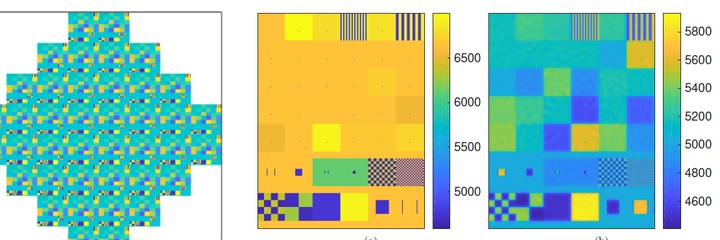
Working with collaborators, Brian Salazar developed a die-scale simulation that resolves the pad’s contact with the evolving wafer topography, uses measured pad surface scans to represent asperities, and predicts planarization efficiency for arbitrary layouts. The model lets engineers compare pad designs, including segmented pads that could be made by additive manufacturing, before they are fabricated. A companion method extracts localized removal laws from measured surfaces. The work received the Best Poster Award at the 2019 International Conference on Planarization Technology, and our GDS Analyzer tool on nanoHUB analyzes chip layout files to provide model inputs. The approach is a direct descendant of our nanoimprint simulation methods.
Banner: the length scales of CMP (left) and simulated post-polish thickness maps for a test die under different pad designs (center and right). From B. Salazar’s Ph.D. research.
Key publications
[C19] B. Salazar, R. Kakireddy, S. Jayanth, A. Chockalingam, R. Bajaj, and H. Taylor, “A new method for characterizing CMP’s localized removal laws using a die-scale modeling approach with measured surfaces,” in Proc. International Conference on Planarization Technology, Portland, OR, Sep. 2022.
[C11] B. Salazar, M. Yamamura, R. Kakireddy, S. Jayanth, Z. Yao, A. Chockalingam, R. Bajaj, and H. Taylor, “Die-scale modeling of planarization efficiency using segmented CMP pads: analyzing the effects of asperity topography,” International Conference on Planarization Technology, Hsinchu, Taiwan, Sep. 2019 (Best Poster Award).
[NC54] B. Salazar, R. Kakireddy, S. Jayanth, A. Chockalingam, R. Bajaj, and H. Taylor, “Computational modeling of CMP pads: analyzing the pad geometry’s impact on planarization efficiency,” 239th Electrochemical Society Meeting, May 2021.
[NC41] B. Salazar and H. Taylor, “Computational modeling of segmented CMP pads: planarization efficiency prediction using measured surface scans,” 22nd International Symposium on Chemical-Mechanical Planarization, Lake Placid, NY, Aug. 2018.
[S3] J. Spitz, J. Qiu, B. Salazar, and H. Taylor, “GDS Analyzer,” nanoHUB, 2019.